Ordering number : ENA1903A ATP613
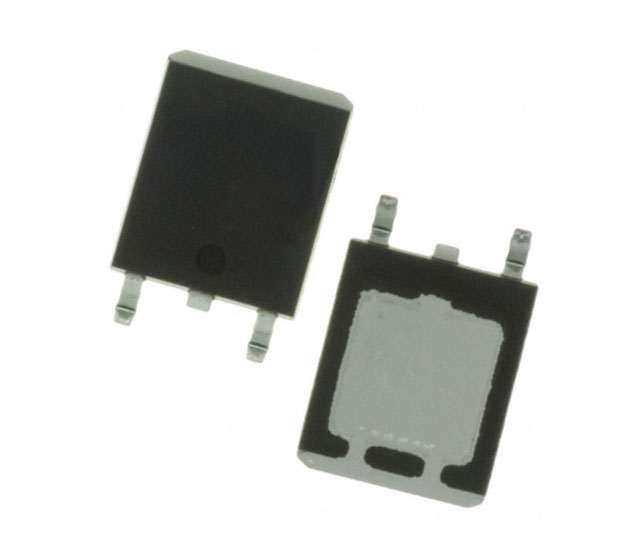
N-Channel Power MOSFET http://onsemi.com 500V, 5.5A, 2Ω, ATPAK
Features
•
•
• Reverse recovery time trr=60ns(typ.)
Input Capacitance Ciss=350pF(typ.)
Halogen free compliance ON-resistance RDS(on)=1.55Ω(typ.)
10V drive •
• Specifications
Absolute Maximum Ratings at Ta=25°C
Parameter Symbol Drain-to-Source Voltage Conditions Ratings VDSS
VGSS Gate-to-Source Voltage
Drain Current (DC) Unit
500 V ±30 V 5.5 A 19 A PW≤10μs, duty cycle≤1% Source-to-Drain Diode Forward Current (DC) ID
IDP
IS Source-to-Drain Diode Forward Current (Pulse) ISP PW≤10μs, duty cycle≤1% Allowable Power Dissipation PD
Tch Tc=25°C Channel Temperature
Storage Temperature Tstg -55 to +150 °C Avalanche Energy (Single Pulse) *1 EAS
IAV 93 mJ 5.5 A Drain Current (Pulse) Avalanche Current *2 5.5 A 19 A 70 W 150 °C Note : *1 VDD=99V, L=5mH, IAV=5.5A (Fig.1)
*2 L≤5mH, Single pulse
Stresses exceeding Maximum Ratings may damage the device. Maximum Ratings are stress ratings only. Functional operation above the Recommended Operating
Conditions is not implied. Extended exposure to stresses above the Recommended Operating Conditions may affect device reliability. Package Dimensions Product & Package Information unit : mm (typ) …