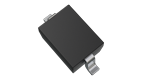
CUS10S30
Schottky Barrier Diode Silicon Epitaxial CUS10S30
1. Applications
• High-Speed Switching 2. Packaging and Internal Circuit 1: Cathode
2: Anode USC 3. Absolute Maximum Ratings (Note) (Unless otherwise specified, Ta = 25 )
Characteristics
Peak reverse voltage
Reverse voltage
Average rectified current
Non-repetitive peak forward surge current Symbol Note Rating Unit VRM 30 V VR 20 IO (Note 1) 1.0 IFSM (Note 2) 5 Junction temperature Tj 125 Storage temperature Tstg -55 to 125 A Note: Using continuously under heavy loads (e.g. the application of high temperature/current/voltage and the
significant change in temperature, etc.) may cause this product to decrease in the reliability significantly even
if the operating conditions (i.e. operating temperature/current/voltage, etc.) are within the absolute maximum
ratings.
Please design the appropriate reliability upon reviewing the Toshiba Semiconductor Reliability Handbook
("Handling Precautions"/"Derating Concept and Methods") and individual reliability data (i.e. reliability test
report and estimated failure rate, etc).
Note 1: Mounted on an FR4 board.
(25.4 mm × 25.4 mm × 1.6 mm, Cu Pad: 645 mm2)
Note 2: Measured with a 10 ms pulse. Start of commercial production 1 2013-09
2014-04-07
Rev.2.0 CUS10S30
4. Electrical Characteristics (Unless otherwise specified, Ta = 25 )
Characteristics Symbol Test Condition Min Typ. Max Unit Forward voltage VF(1) IF = 0.1 A (Pulse test) 0.23 V Forward voltage VF(2) IF = 0.5 A (Pulse test) 0.31 V Forward voltage VF(3) IF = 1 A (Pulse test) 0.37 0.45 V Reverse current IR VR = 30 V (Pulse test) 0.2 0.5 mA Total capacitance Ct VR = 0 V, f = 1 MHz 135 pF 5. Marking Fig. 5.1 Marking Marking Code Part Number 8C CUS10S30 6. Usage Considerations …