Datasheet Texas Instruments SN74LVC1G18 — Datenblatt
| Hersteller | Texas Instruments |
| Serie | SN74LVC1G18 |
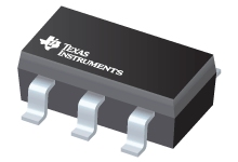
Einer von zwei nicht invertierenden Demultiplexern mit abgewähltem 3-Zustands-Ausgang
Datenblätter
1-of-2 Noninverting Demultiplexer With 3-State Deselected Output datasheet
PDF, 1.2 Mb, Revision: K, Datei veröffentlicht: Jul 19, 2012
Auszug aus dem Dokument
Status
| SN74LVC1G18DBVR | SN74LVC1G18DBVRG4 | SN74LVC1G18DCKR | SN74LVC1G18DCKRE4 | SN74LVC1G18DCKRG4 | SN74LVC1G18DRYR | SN74LVC1G18DSFR | SN74LVC1G18YZPR | |
|---|---|---|---|---|---|---|---|---|
| Lifecycle Status | Active (Recommended for new designs) | Active (Recommended for new designs) | Active (Recommended for new designs) | Active (Recommended for new designs) | Active (Recommended for new designs) | Active (Recommended for new designs) | Active (Recommended for new designs) | Active (Recommended for new designs) |
| Manufacture's Sample Availability | Yes | Yes | Yes | Yes | Yes | Yes | Yes | Yes |
Verpackung
| SN74LVC1G18DBVR | SN74LVC1G18DBVRG4 | SN74LVC1G18DCKR | SN74LVC1G18DCKRE4 | SN74LVC1G18DCKRG4 | SN74LVC1G18DRYR | SN74LVC1G18DSFR | SN74LVC1G18YZPR | |
|---|---|---|---|---|---|---|---|---|
| N | 1 | 2 | 3 | 4 | 5 | 6 | 7 | 8 |
| Pin | 6 | 6 | 6 | 6 | 6 | 6 | 6 | 6 |
| Package Type | DBV | DBV | DCK | DCK | DCK | DRY | DSF | YZP |
| Industry STD Term | SOT-23 | SOT-23 | SOT-SC70 | SOT-SC70 | SOT-SC70 | USON | X2SON | DSBGA |
| JEDEC Code | R-PDSO-G | R-PDSO-G | R-PDSO-G | R-PDSO-G | R-PDSO-G | R-PDSO-N | S-PDSO-N | R-XBGA-N |
| Package QTY | 3000 | 3000 | 3000 | 3000 | 3000 | 5000 | 5000 | 3000 |
| Carrier | LARGE T&R | LARGE T&R | LARGE T&R | LARGE T&R | LARGE T&R | LARGE T&R | LARGE T&R | LARGE T&R |
| Device Marking | C18R | C18R | CJF | CJK | CJK | CJ | CJ | CJN |
| Width (mm) | 1.6 | 1.6 | 1.25 | 1.25 | 1.25 | 1 | 1 | .9 |
| Length (mm) | 2.9 | 2.9 | 2 | 2 | 2 | 1.45 | 1 | 1.5 |
| Thickness (mm) | 1.2 | 1.2 | .9 | .9 | .9 | .5 | .35 | 2 |
| Pitch (mm) | .95 | .95 | .65 | .65 | .65 | .5 | .35 | .5 |
| Max Height (mm) | 1.45 | 1.45 | 1.1 | 1.1 | 1.1 | .6 | .4 | .5 |
| Mechanical Data | Herunterladen | Herunterladen | Herunterladen | Herunterladen | Herunterladen | Herunterladen | Herunterladen | Herunterladen |
Parameter
| Parameters / Models | SN74LVC1G18DBVR | SN74LVC1G18DBVRG4 | SN74LVC1G18DCKR | SN74LVC1G18DCKRE4 | SN74LVC1G18DCKRG4 | SN74LVC1G18DRYR | SN74LVC1G18DSFR | SN74LVC1G18YZPR |
|---|---|---|---|---|---|---|---|---|
| 3-State Output | No | No | No | No | No | No | No | No |
| Bits | 1 | 1 | 1 | 1 | 1 | 1 | 1 | 1 |
| F @ Nom Voltage(Max), Mhz | 150 | 150 | 150 | 150 | 150 | 150 | 150 | 150 |
| Gate Type | DECODER/DEMUX | DECODER/DEMUX | DECODER/DEMUX | DECODER/DEMUX | DECODER/DEMUX | DECODER/DEMUX | DECODER/DEMUX | DECODER/DEMUX |
| ICC @ Nom Voltage(Max), mA | 0.01 | 0.01 | 0.01 | 0.01 | 0.01 | 0.01 | 0.01 | 0.01 |
| Logic | True | True | True | True | True | True | True | True |
| Operating Temperature Range, C | -40 to 85 | -40 to 85 | -40 to 85 | -40 to 85 | -40 to 85 | -40 to 85 | -40 to 85 | -40 to 85 |
| Output Drive (IOL/IOH)(Max), mA | 32/-32 | 32/-32 | 32/-32 | 32/-32 | 32/-32 | 32/-32 | 32/-32 | 32/-32 |
| Package Group | SOT-23 | SOT-23 | SC70 | SC70 | SC70 | SON | SON | DSBGA |
| Package Size: mm2:W x L, PKG | 6SOT-23: 8 mm2: 2.8 x 2.9(SOT-23) | 6SOT-23: 8 mm2: 2.8 x 2.9(SOT-23) | 6SC70: 4 mm2: 2.1 x 2(SC70) | 6SC70: 4 mm2: 2.1 x 2(SC70) | 6SC70: 4 mm2: 2.1 x 2(SC70) | See datasheet (SON) | See datasheet (SON) | See datasheet (DSBGA) |
| Rating | Catalog | Catalog | Catalog | Catalog | Catalog | Catalog | Catalog | Catalog |
| Schmitt Trigger | No | No | No | No | No | No | No | No |
| Special Features | Ioff,down translation to Vcc,low power | Ioff,down translation to Vcc,low power | Ioff,down translation to Vcc,low power | Ioff,down translation to Vcc,low power | Ioff,down translation to Vcc,low power | Ioff,down translation to Vcc,low power | Ioff,down translation to Vcc,low power | Ioff,down translation to Vcc,low power |
| Sub-Family | Decoder/Encoder/Multiplexer | Decoder/Encoder/Multiplexer | Decoder/Encoder/Multiplexer | Decoder/Encoder/Multiplexer | Decoder/Encoder/Multiplexer | Decoder/Encoder/Multiplexer | Decoder/Encoder/Multiplexer | Decoder/Encoder/Multiplexer |
| Technology Family | LVC | LVC | LVC | LVC | LVC | LVC | LVC | LVC |
| VCC(Max), V | 5.5 | 5.5 | 5.5 | 5.5 | 5.5 | 5.5 | 5.5 | 5.5 |
| VCC(Min), V | 1.65 | 1.65 | 1.65 | 1.65 | 1.65 | 1.65 | 1.65 | 1.65 |
| Voltage(Nom), V | 1.8,2.5,3.3,5 | 1.8,2.5,3.3,5 | 1.8,2.5,3.3,5 | 1.8,2.5,3.3,5 | 1.8,2.5,3.3,5 | 1.8,2.5,3.3,5 | 1.8,2.5,3.3,5 | 1.8,2.5,3.3,5 |
| tpd @ Nom Voltage(Max), ns | 9.3,5,4.2,3.2 | 9.3,5,4.2,3.2 | 9.3,5,4.2,3.2 | 9.3,5,4.2,3.2 | 9.3,5,4.2,3.2 | 9.3,5,4.2,3.2 | 9.3,5,4.2,3.2 | 9.3,5,4.2,3.2 |
Öko-Plan
| SN74LVC1G18DBVR | SN74LVC1G18DBVRG4 | SN74LVC1G18DCKR | SN74LVC1G18DCKRE4 | SN74LVC1G18DCKRG4 | SN74LVC1G18DRYR | SN74LVC1G18DSFR | SN74LVC1G18YZPR | |
|---|---|---|---|---|---|---|---|---|
| RoHS | Compliant | Compliant | Compliant | Compliant | Compliant | Compliant | Compliant | Compliant |
Anwendungshinweise
- LVC Characterization InformationPDF, 114 Kb, Datei veröffentlicht: Dec 1, 1996
This document provides characterization information about low-voltage logic (LVL) that operates from a 3.3-V power supply. It addresses the issues of interfacing to 5-V logic ac performance power considerations input and output characteristics and signal integrity for this family of devices. - Use of the CMOS Unbuffered Inverter in Oscillator CircuitsPDF, 796 Kb, Datei veröffentlicht: Nov 6, 2003
CMOS devices have a high input impedance high gain and high bandwidth. These characteristics are similar to ideal amplifier characteristics and hence a CMOS buffer or inverter can be used in an oscillator circuit in conjunction with other passive components. Now CMOS oscillator circuits are widely used in high-speed applications because they are economical easy to use and take significantly
Modellreihe
Serie: SN74LVC1G18 (8)
Herstellerklassifikation
- Semiconductors> Logic> Little Logic