Datasheet Texas Instruments OPA684 — Datenblatt
| Hersteller | Texas Instruments |
| Serie | OPA684 |
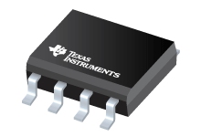
Stromrückkopplungs-Operationsverstärker mit geringem Stromverbrauch und Deaktivierung
Datenblätter
Low-Power, Current Feedback Operational Amplifier With Disable datasheet
PDF, 1.1 Mb, Revision: D, Datei veröffentlicht: Jun 19, 2009
Auszug aus dem Dokument
Preise
Status
| OPA684ID | OPA684IDBVR | OPA684IDBVRG4 | OPA684IDBVT | OPA684IDBVTG4 | OPA684IDG4 | OPA684IDR | OPA684IDRG4 | |
|---|---|---|---|---|---|---|---|---|
| Lifecycle Status | Active (Recommended for new designs) | Active (Recommended for new designs) | Active (Recommended for new designs) | Active (Recommended for new designs) | Active (Recommended for new designs) | Active (Recommended for new designs) | Active (Recommended for new designs) | Active (Recommended for new designs) |
| Manufacture's Sample Availability | Yes | No | Yes | No | Yes | No | Yes | Yes |
Verpackung
| OPA684ID | OPA684IDBVR | OPA684IDBVRG4 | OPA684IDBVT | OPA684IDBVTG4 | OPA684IDG4 | OPA684IDR | OPA684IDRG4 | |
|---|---|---|---|---|---|---|---|---|
| N | 1 | 2 | 3 | 4 | 5 | 6 | 7 | 8 |
| Pin | 8 | 6 | 6 | 6 | 6 | 8 | 8 | 8 |
| Package Type | D | DBV | DBV | DBV | DBV | D | D | D |
| Industry STD Term | SOIC | SOT-23 | SOT-23 | SOT-23 | SOT-23 | SOIC | SOIC | SOIC |
| JEDEC Code | R-PDSO-G | R-PDSO-G | R-PDSO-G | R-PDSO-G | R-PDSO-G | R-PDSO-G | R-PDSO-G | R-PDSO-G |
| Package QTY | 75 | 3000 | 3000 | 250 | 250 | 75 | 2500 | 2500 |
| Carrier | TUBE | LARGE T&R | LARGE T&R | SMALL T&R | SMALL T&R | TUBE | LARGE T&R | LARGE T&R |
| Device Marking | OPA | B84 | B84 | B84 | B84 | OPA | 684 | OPA |
| Width (mm) | 3.91 | 1.6 | 1.6 | 1.6 | 1.6 | 3.91 | 3.91 | 3.91 |
| Length (mm) | 4.9 | 2.9 | 2.9 | 2.9 | 2.9 | 4.9 | 4.9 | 4.9 |
| Thickness (mm) | 1.58 | 1.2 | 1.2 | 1.2 | 1.2 | 1.58 | 1.58 | 1.58 |
| Pitch (mm) | 1.27 | .95 | .95 | .95 | .95 | 1.27 | 1.27 | 1.27 |
| Max Height (mm) | 1.75 | 1.45 | 1.45 | 1.45 | 1.45 | 1.75 | 1.75 | 1.75 |
| Mechanical Data | Herunterladen | Herunterladen | Herunterladen | Herunterladen | Herunterladen | Herunterladen | Herunterladen | Herunterladen |
Parameter
| Parameters / Models | OPA684ID | OPA684IDBVR | OPA684IDBVRG4 | OPA684IDBVT | OPA684IDBVTG4 | OPA684IDG4 | OPA684IDR | OPA684IDRG4 |
|---|---|---|---|---|---|---|---|---|
| 2nd Harmonic, dBc | 67 | 67 | 67 | 67 | 67 | 67 | 67 | 67 |
| 3rd Harmonic, dBc | 70 | 70 | 70 | 70 | 70 | 70 | 70 | 70 |
| @ MHz | 5 | 5 | 5 | 5 | 5 | 5 | 5 | 5 |
| Acl, min spec gain, V/V | 1 | 1 | 1 | 1 | 1 | 1 | 1 | 1 |
| Additional Features | Shutdown | Shutdown | Shutdown | Shutdown | Shutdown | Shutdown | Shutdown | Shutdown |
| Architecture | Bipolar,Current FB | Bipolar,Current FB | Bipolar,Current FB | Bipolar,Current FB | Bipolar,Current FB | Bipolar,Current FB | Bipolar,Current FB | Bipolar,Current FB |
| BW @ Acl, MHz | 210 | 210 | 210 | 210 | 210 | 210 | 210 | 210 |
| CMRR(Min), dB | 53 | 53 | 53 | 53 | 53 | 53 | 53 | 53 |
| CMRR(Typ), dB | 60 | 60 | 60 | 60 | 60 | 60 | 60 | 60 |
| GBW(Typ), MHz | 210 | 210 | 210 | 210 | 210 | 210 | 210 | 210 |
| Input Bias Current(Max), pA | 10000000 | 10000000 | 10000000 | 10000000 | 10000000 | 10000000 | 10000000 | 10000000 |
| Iq per channel(Max), mA | 1.8 | 1.8 | 1.8 | 1.8 | 1.8 | 1.8 | 1.8 | 1.8 |
| Iq per channel(Typ), mA | 1.7 | 1.7 | 1.7 | 1.7 | 1.7 | 1.7 | 1.7 | 1.7 |
| Number of Channels | 1 | 1 | 1 | 1 | 1 | 1 | 1 | 1 |
| Offset Drift(Typ), uV/C | 12 | 12 | 12 | 12 | 12 | 12 | 12 | 12 |
| Operating Temperature Range, C | -40 to 85 | -40 to 85 | -40 to 85 | -40 to 85 | -40 to 85 | -40 to 85 | -40 to 85 | -40 to 85 |
| Output Current(Typ), mA | 120 | 120 | 120 | 120 | 120 | 120 | 120 | 120 |
| Package Group | SOIC | SOT-23 | SOT-23 | SOT-23 | SOT-23 | SOIC | SOIC | SOIC |
| Package Size: mm2:W x L, PKG | 8SOIC: 29 mm2: 6 x 4.9(SOIC) | 6SOT-23: 8 mm2: 2.8 x 2.9(SOT-23) | 6SOT-23: 8 mm2: 2.8 x 2.9(SOT-23) | 6SOT-23: 8 mm2: 2.8 x 2.9(SOT-23) | 6SOT-23: 8 mm2: 2.8 x 2.9(SOT-23) | 8SOIC: 29 mm2: 6 x 4.9(SOIC) | 8SOIC: 29 mm2: 6 x 4.9(SOIC) | 8SOIC: 29 mm2: 6 x 4.9(SOIC) |
| Rail-to-Rail | No | No | No | No | No | No | No | No |
| Rating | Catalog | Catalog | Catalog | Catalog | Catalog | Catalog | Catalog | Catalog |
| Slew Rate(Typ), V/us | 820 | 820 | 820 | 820 | 820 | 820 | 820 | 820 |
| Total Supply Voltage(Max), +5V=5, +/-5V=10 | 12 | 12 | 12 | 12 | 12 | 12 | 12 | 12 |
| Total Supply Voltage(Min), +5V=5, +/-5V=10 | 5 | 5 | 5 | 5 | 5 | 5 | 5 | 5 |
| Vn at 1kHz(Typ), nV/rtHz | 3.7 | 3.7 | 3.7 | 3.7 | 3.7 | 3.7 | 3.7 | 3.7 |
| Vn at Flatband(Typ), nV/rtHz | 3.7 | 3.7 | 3.7 | 3.7 | 3.7 | 3.7 | 3.7 | 3.7 |
| Vos (Offset Voltage @ 25C)(Max), mV | 3.5 | 3.5 | 3.5 | 3.5 | 3.5 | 3.5 | 3.5 | 3.5 |
Öko-Plan
| OPA684ID | OPA684IDBVR | OPA684IDBVRG4 | OPA684IDBVT | OPA684IDBVTG4 | OPA684IDG4 | OPA684IDR | OPA684IDRG4 | |
|---|---|---|---|---|---|---|---|---|
| RoHS | Compliant | Compliant | Compliant | Compliant | Compliant | Compliant | Compliant | Compliant |
Anwendungshinweise
- Considerations for High-Gain Multistage DesignsPDF, 347 Kb, Datei veröffentlicht: May 13, 2013
- Making the Most of a Low-Power, High-Speed Operational AmplifierPDF, 221 Kb, Datei veröffentlicht: Nov 22, 2009
High-speed, high-performance operational amplifiers tend to be associated with high power dissipation. This application note compares the relative performance of several low-power, high-speed operational amplifiers and describes trade-offs to balance performance with low quiescent power dissipation. - A Numerical Solution to an Analog ProblemPDF, 210 Kb, Datei veröffentlicht: Apr 25, 2010
In order to derive a solution for an analog circuit problem, it is often useful to develop a model. This approach is generally accepted as developing an analytical model. However, finding the analytical solution is not always practical or possible as a result of higher-degree polynomials that require further resolution, or because of the time needed to develop the solution completely. In these sit - Current Feedback Amplifiers: Review, Stability Analysis, and ApplicationsPDF, 53 Kb, Datei veröffentlicht: Nov 20, 2000
The majority of op amp circuits are closed-loop feedback systems that implement classical control theory analysis. Analog designers are comfortable with Voltage FeedBack (VFB) op amps in a closed-loop system and are familiar with the ideal op amp approximations feedback permit. This application bulletin will demonstrate how CFB op amps can be analyzed in a similar fashion. Once the closed-loop sim - Stabilizing Current-Feedback Op Amps While Optimizing Circuit PerformancePDF, 280 Kb, Datei veröffentlicht: Apr 28, 2004
Optimizing a circuit design with a current-feedback (CFB) op amp is a relatively straightforward task, once one understands how CFB op amps achieve stability. This application note explains a 2nd-order CFB model so that any designer can better understand the flexibility of the CFB op amp. This report also discusses stability analysis, the effects of parasitic components due to PCBs, optimization - Expanding the usability of current-feedback amplifiersPDF, 215 Kb, Datei veröffentlicht: Feb 28, 2005
- Active filters using current-feedback amplifiersPDF, 227 Kb, Datei veröffentlicht: Feb 25, 2005
- RLC Filter Design for ADC Interface Applications (Rev. A)PDF, 299 Kb, Revision: A, Datei veröffentlicht: May 13, 2015
As high performance Analog-to-Digital Converters (ADCs) continue to improve in their performance, the last stage interface from the final amplifier into the converter inputs becomes a critical element in the system design if the full converter dynamic range is desired. This application note describes the performance and design equations for a simple passive 2nd-order filter used successfully in AD - Wideband Complementary Current Output DAC Single-Ended InterfacePDF, 597 Kb, Datei veröffentlicht: Jun 21, 2005
High-speed digital-to-analog converters (DACs) most often use a transformer-coupled output stage. In applications where this configuration is not practical, a single op ampdifferential to single-ended stage has often been used. This application note steps through the exact design equations required to achieve gain matching from each output as well as a matched input impedance to each of the DA - ADS5500, OPA695: PC Board Layout for Low Distortion High-Speed ADC DriversPDF, 273 Kb, Datei veröffentlicht: Apr 22, 2004
Once an analog-to-digital converter (ADC) and a driver/interface have been selected for a given application, the next step to achieving excellent performance is laying out the printed circuit board (PCB) that will support the application. This application report describes several techniques for optimizing a high-speed, 14-bit performance, differential driver PCB layout using a wideband operation - Measuring Board Parasitics in High-Speed Analog DesignPDF, 134 Kb, Datei veröffentlicht: Jul 7, 2003
Successful circuit designs using high-speed amplifiers can depend upon understanding and identifying parasitic PCB components. Simulating a design while including PCB parasitics can protect against unpleasant production surprises. This application report discusses an easy method for measuring parasitic components in a prototype or final PC board design by using a standard oscilloscope and low freq - Noise Analysis for High Speed Op Amps (Rev. A)PDF, 256 Kb, Revision: A, Datei veröffentlicht: Jan 17, 2005
As system bandwidths have increased an accurate estimate of the noise contribution for each element in the signal channel has become increasingly important. Many designers are not however particularly comfortable with the calculations required to predict the total noise for an op amp or in the conversions between the different descriptions of noise. Considerable inconsistency between manufactu
Modellreihe
Serie: OPA684 (8)
Herstellerklassifikation
- Semiconductors> Amplifiers> Operational Amplifiers (Op Amps)> High-Speed Op Amps (>=50MHz)