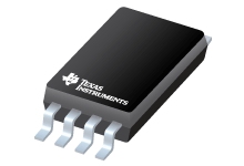
Datasheet Texas Instruments CDCLVC1104 — Datenblatt
| Hersteller | Texas Instruments |
| Serie | CDCLVC1104 |

Low Jitter, 1: 4 LVCMOS Fan-Out-Taktpuffer
Datenblätter
CDCLVC11xx 3.3-V and 2.5-V LVCMOS High-Performance Clock Buffer Family datasheet
PDF, 1.6 Mb, Revision: B, Datei veröffentlicht: Feb 24, 2017
Auszug aus dem Dokument
Status
| CDCLVC1104PW | CDCLVC1104PWR | |
|---|---|---|
| Lifecycle Status | Active (Recommended for new designs) | Active (Recommended for new designs) |
| Manufacture's Sample Availability | Yes | Yes |
Verpackung
| CDCLVC1104PW | CDCLVC1104PWR | |
|---|---|---|
| N | 1 | 2 |
| Pin | 8 | 8 |
| Package Type | PW | PW |
| Industry STD Term | TSSOP | TSSOP |
| JEDEC Code | R-PDSO-G | R-PDSO-G |
| Package QTY | 150 | 2000 |
| Carrier | TUBE | LARGE T&R |
| Device Marking | C9C4 | C9C4 |
| Width (mm) | 4.4 | 4.4 |
| Length (mm) | 3 | 3 |
| Thickness (mm) | 1 | 1 |
| Pitch (mm) | .65 | .65 |
| Max Height (mm) | 1.2 | 1.2 |
| Mechanical Data | Herunterladen | Herunterladen |
Parameter
| Parameters / Models | CDCLVC1104PW | CDCLVC1104PWR |
|---|---|---|
| Additive RMS Jitter(Typ), fs | 70 | 70 |
| Input Frequency(Max), MHz | 250 | 250 |
| Input Level | LVCMOS | LVCMOS |
| Number of Outputs | 4 | 4 |
| Operating Temperature Range, C | -40 to 85 | -40 to 85 |
| Output Frequency(Max), MHz | 250 | 250 |
| Output Level | LVCMOS | LVCMOS |
| Package Group | TSSOP | TSSOP |
| Package Size: mm2:W x L, PKG | 8TSSOP: 19 mm2: 6.4 x 3(TSSOP) | 8TSSOP: 19 mm2: 6.4 x 3(TSSOP) |
| Rating | Catalog | Catalog |
| VCC Out, V | 2.5,3.3 | 2.5,3.3 |
Öko-Plan
| CDCLVC1104PW | CDCLVC1104PWR | |
|---|---|---|
| RoHS | Compliant | Compliant |
Anwendungshinweise
- How to Apply 1.8-V Signals to 3.3-V CDCLVC11xx Fanout Clock BufferPDF, 518 Kb, Datei veröffentlicht: Nov 30, 2010
The CDCLVC11xx buffer family from Texas Instruments has a nominal voltage supply of 2.5 V and 3.3 V. With the simple employment of an external RC network, this family of devices can handle incoming signals whose voltage levels go up to 1.8 V. This application report explains how to implement this network and dimension its discrete components, without impacting the specifications of additive ji
Modellreihe
Serie: CDCLVC1104 (2)
Herstellerklassifikation
- Semiconductors> Clock and Timing> Clock Buffers> Single-Ended