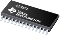
Datasheet Texas Instruments ADS574JP-2 — Datenblatt
| Hersteller | Texas Instruments |
| Serie | ADS574 |
| Artikelnummer | ADS574JP-2 |
Datenblätter
Datasheet
Anwendungshinweise
- Analog-to-Digital Converter Grounding Practices Affect System Performance (Rev. A)PDF, 69 Kb, Revision: A, Datei veröffentlicht: May 18, 2015
- CDAC Architecture Gives ADC574 Pinout /Sampling, Low Power, New Input RangesPDF, 54 Kb, Datei veröffentlicht: Sep 27, 2000
This application note compares basic current-mode successive approximation A/Ds with CDAC-based architectures, and shows how adding a resistor divider network to the CDAC input permits the Burr-Brown ADS574 and ADS774 to fit existing ADC574 sockets. It then goes on to descibe some new analog input voltage ranges available on these parts due to the resistor network and CDAC approach. - A Glossary of Analog-to-Digital Specifications and Performance Characteristics (Rev. B)PDF, 425 Kb, Revision: B, Datei veröffentlicht: Oct 9, 2011
This glossary is a collection of the definitions of Texas Instruments' Delta-Sigma (О”ОЈ), successive approximation register (SAR), and pipeline analog-to-digital (A/D) converter specifications and performance characteristics. Although there is a considerable amount of detail in this document, the product data sheet for a particular product specification is the best and final reference. - Interleaving Analog-to-Digital ConvertersPDF, 64 Kb, Datei veröffentlicht: Oct 2, 2000
It is tempting when pushing the limits of analog-to-digital conversion to consider interleaving two or more converters to increase the sample rate. However, such designs must take into consideration several possible sources of error. - Complete Temp Data Acquisition System From a Single +5V SupplyPDF, 68 Kb, Datei veröffentlicht: Oct 2, 2000
The CMOS ADS574 and ADS774 are drop-in replacements for industry standard ADC574 analog-to-digital converter, offering lower power and the capability to operate from a single +5V supply. The switched capacitor array architecture (CDAC), with the input resistor divider network to provide ADC574 input ranges, also allow the new parts to handle additional input ranges, including a 0V to 5V range. Thi - Determining Minimum Acquisition Times for SAR ADCs, part 1 (Rev. A)PDF, 227 Kb, Revision: A, Datei veröffentlicht: Nov 10, 2010
This application report analyzes a simple method for calculating minimum acquisition times for successive-approximation register analog-to-digital converters (SAR ADCs). The input structure of the ADC is examined along with the driving circuit. The voltage on the sampling capacitor is then determined for the case when a step function is applied to the input of the driving circuit. Three different - What Designers Should Know About Data Converter DriftPDF, 95 Kb, Datei veröffentlicht: Oct 2, 2000
Exactly how inaccurate will a change in temperature make an analog-to-digital or digital-to-analog converter? As designers are well aware, a 12-bit device may provide a much lower accuracy at its operating-temperature extremes, perhaps only to 9 or even 8 bits. But for lack of more precise knowledge, many play it safe (and expensive) and overspecify. - Principles of Data Acquisition and Conversion (Rev. A)PDF, 132 Kb, Revision: A, Datei veröffentlicht: Apr 16, 2015
- Determining Minimum Acquisition Times for SAR ADCs, part 2PDF, 215 Kb, Datei veröffentlicht: Mar 17, 2011
The input structure circuit of a successive-approximation register analog-to-digital converter (SAR ADC) incombination with the driving circuit forms a transfer function that can be used to determine minimum acquisition times for different types of applied input signals. This application report, which builds on Determining Minimum Acquisition Times for SAR ADCs When a Step Function is Applied to
Modellreihe
Serie: ADS574 (7)
- ADS574AU ADS574AU/1K ADS574JP-2 ADS574JU ADS574JU/1K ADS574KPG4 ADS574KU-2
Herstellerklassifikation
- Semiconductors > Data Converters > Analog to Digital Converter > Precision ADC (<=10MSPS)
Andere Namen:
ADS574JP2, ADS574JP 2