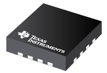
Datasheet Texas Instruments THS4541IRGTR — Datenblatt
| Hersteller | Texas Instruments |
| Serie | THS4541 |
| Artikelnummer | THS4541IRGTR |

Hochgeschwindigkeits-Differenzial-E / A-Verstärker 16-VQFN -40 bis 125
Datenblätter
THS4541 Negative Rail Input, Rail-to-Rail Output, Precision, 850-MHz Fully Differential Amplifier datasheet
PDF, 2.2 Mb, Revision: A, Datei veröffentlicht: Sep 30, 2014
Auszug aus dem Dokument
Preise
Status
| Lifecycle Status | Active (Recommended for new designs) |
| Manufacture's Sample Availability | No |
Verpackung
| Pin | 16 |
| Package Type | RGT |
| Industry STD Term | VQFN |
| JEDEC Code | S-PQFP-N |
| Package QTY | 3000 |
| Carrier | LARGE T&R |
| Device Marking | HS4541 |
| Width (mm) | 3 |
| Length (mm) | 3 |
| Thickness (mm) | .9 |
| Pitch (mm) | .5 |
| Max Height (mm) | 1 |
| Mechanical Data | Herunterladen |
Parameter
| 2nd Harmonic | 140 dBc |
| 3rd Harmonic | 140 dBc |
| @ MHz | 0.1 |
| Acl, min spec gain | 1 V/V |
| Additional Features | Shutdown |
| Architecture | Fully Differential,Voltage FB |
| BW @ Acl | 620 MHz |
| CMRR(Min) | 85 dB |
| CMRR(Typ) | 100 dB |
| GBW(Typ) | 850 MHz |
| Input Bias Current(Max) | 13000000 pA |
| Iq per channel(Max) | 10.5 mA |
| Iq per channel(Typ) | 10.1 mA |
| Number of Channels | 1 |
| Offset Drift(Typ) | 0.5 uV/C |
| Operating Temperature Range | -40 to 125 C |
| Output Current(Typ) | 100 mA |
| Package Group | VQFN |
| Package Size: mm2:W x L | 16VQFN: 9 mm2: 3 x 3(VQFN) PKG |
| Rail-to-Rail | In to V-,Out |
| Rating | Catalog |
| Slew Rate(Typ) | 1500 V/us |
| Total Supply Voltage(Max) | 5.4 +5V=5, +/-5V=10 |
| Total Supply Voltage(Min) | 2.7 +5V=5, +/-5V=10 |
| Vn at 1kHz(Typ) | 33 nV/rtHz |
| Vn at Flatband(Typ) | 2.2 nV/rtHz |
| Vos (Offset Voltage @ 25C)(Max) | 0.45 mV |
Öko-Plan
| RoHS | Compliant |
Design Kits und Evaluierungsmodule
- Evaluation Modules & Boards: THS4541RGTEVM
THS4541 Evaluation Module in RGT Package
Lifecycle Status: Active (Recommended for new designs) - Evaluation Modules & Boards: DEV-ADC34J22
DEV-ADC34J22 Evaluation Module
Lifecycle Status: Active (Recommended for new designs)
Anwendungshinweise
- Input impedance matching with fully differential amplifiersPDF, 643 Kb, Datei veröffentlicht: Oct 22, 2008
- Using single-supply fully diff. amps with neg. input voltages to drive ADCsPDF, 105 Kb, Datei veröffentlicht: Nov 15, 2010
- Design for a Wideband Differential Transimpedance DAC Output (Rev. A)PDF, 438 Kb, Revision: A, Datei veröffentlicht: Oct 17, 2016
High-speed digital-to-analog converters commonly offer a complementary current output signal. Most output interface implementations use either a resistive load and/or a transformer to convert this current source signal to a voltage. Where a dc-coupled interface is required, a carefully designed differential transimpedance stage can offer an attractive alternative. Design considerations and options - Noise Analysis for High Speed Op Amps (Rev. A)PDF, 256 Kb, Revision: A, Datei veröffentlicht: Jan 17, 2005
As system bandwidths have increased an accurate estimate of the noise contribution for each element in the signal channel has become increasingly important. Many designers are not however particularly comfortable with the calculations required to predict the total noise for an op amp or in the conversions between the different descriptions of noise. Considerable inconsistency between manufactu
Modellreihe
Serie: THS4541 (4)
- THS4541IRGTR THS4541IRGTT THS4541IRUNR THS4541IRUNT
Herstellerklassifikation
- Semiconductors > Amplifiers > Operational Amplifiers (Op Amps) > High-Speed Op Amps (>=50MHz)